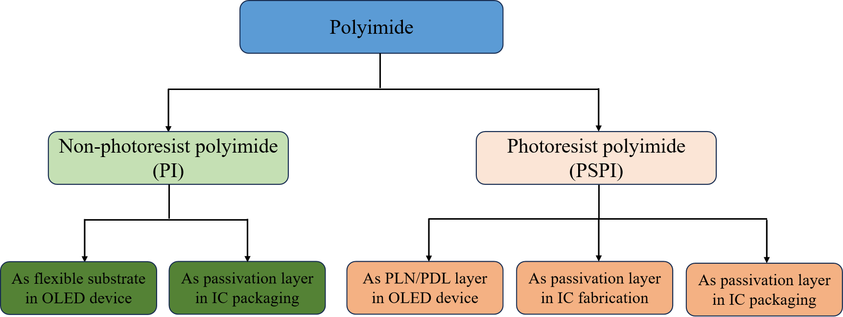
PSPI film was usually regard as an insulation layer in electronics, such as OLED device, IC fabrication and IC packaging. Based on the patterning request of PSPI layer, the usage of PSPI was usually introduced for forming passivation layer based on the technology of photolithography.
2.2.2.1 The application of PSPI used in OLED device
During the manufacturing of OLED device, PSPI was widely used as PLN and PDL due to its photosensitive performance, thermal stability and patterning accuracy.60-61 The application of PSPI not only simplified the process flow, but also directly affected the luminous efficiency, resolution and reliability of OLED display device. Based on its excellent film-forming performance, PSPI could form a uniform thin film through spin coating or spray coating by after a curing process, the surface roughness (Ra) of PSPI layer could reach the value below 0.5nm, which can effectively eliminate the step differences existed in the bottom ITO electrode or TFT array structure and provide a flat substrate for subsequent organic light-emitting layer evaporation. During the high-temperature (about 200-300°C) environment of OLED packaging process, PSPI can still maintain structural stability for resisting acid and alkali corrosion, avoiding chemical reactions with subsequent organic materials.62 For improving the luminescence uniformity and device lifespan of OLED device, PLN layer formed by PSPI can also reduce the uneven thickness of organic luminescent materials causing by the unevenness of the bottom layer and avoid brightness differences in the display screen. The dense molecular structure of PLN layer formed by PSPI can also block the penetration of external water vapor and ions to reduce the dark state current of OLED devices and extend their service life.
The material characteristics of high-precision patterning and mechanical support made it possible for PSPI using as PDL layer in the array structure of OLED display device. Without requiring additional photoresist, PSPI can directly form micrometer level patterns (line width accuracy of 1-3um) based on UV exposure, which could meet the strict requirements of pixel spacing for high-resolution (such as 4K/8K) OLED display device.63 After exposure crosslinking, the unexposed area of negative PSPI dissolves during development process and formed pixel wells perpendicular to the sidewall, which can ensure the precise filling of organic materials during evaporation and avoiding adjacent pixel crosstalk. By using as PDL layer, PSPI layer coulddivide OLED panels into independent red, green, and blue (RGB) sub pixels to prevent mixing of different colored luminescent materials and ensure color purity. During the vapor deposition process of fine metal mask (FMM) technology, the mechanical strength of PSPI can support the bonding accuracy between the mask and the substrate to reduce pixel offset causing by mask deformation.
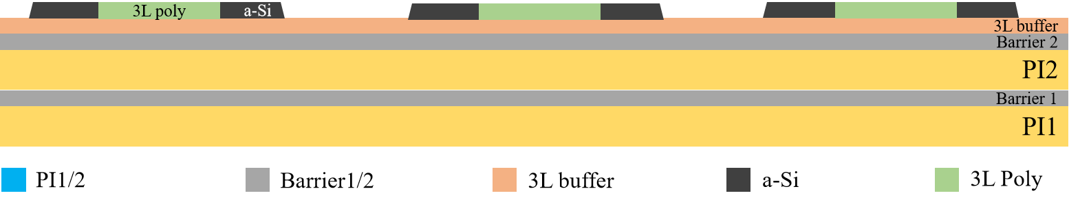
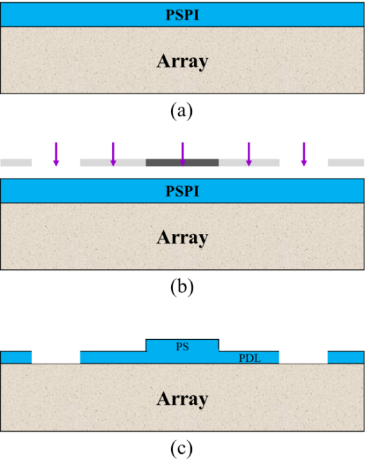
With the development of technology, PSPI was usually used as PLN, PDL and pixel supporting (PS) layer in the foldable flexible OLED device. The PDL and PS layer were usually formed with a technology named half tone mask and the architecture was showed in Figure 6. The half tone mask was made up of three parts, the fully transparent zone, the semipermeable zone and the impermeable zone. During the exposure process, the light can through the fully transparent zone on the mask completely without any loss and reach the surface of PSPI film, and the PSPI film located at the fully transparent zone was removed fully and formed the opening area after the develop process. While, only part of light can through the semipermeable zone on the mask and reach the surface of PSPI film during the process of exposure, the PSPI film located at the semipermeable zone was also removed part thickness and formed the PDL layer after the develop process. Finally, there was no light can through the impermeable zone and reach the surface of PSPI film, the PSPI film located at the impermeable zone remained the fully thickness and formed the PS layer.
Figure 6.
The architecture of PSPI application process flow: (a) PSPI coating, (b) PSPI soft bake, (c) PSPI exposure, (d) PSPI develop, (e) PSPI hard bake. During the preparation of OLED display devices, PSPI was also used to forming the PDL layer and PS based on half-tone mask technology. The principle of half-tone mask was adjusting the exposure dose through the semi transparent area, allowing partial development of the photoresist and forming a thickness gradient slope structure to solve the step coverage problem of the PDL/PS layer.64 The key advantage of half-tone mask was eliminating the flowing of organic material in the climbing area. For example, in the segment difference area (climbing area) of the shading layer (such as metal wiring), the traditional processes of forming PDL usually caused uneven coverage due to the flow of PLN material, which could lead to etching and wire breakage in following process.65 While, the half tone technology could ensure the uniform coverage of PDL layer through gradient slope (controllable inclination angle above 85°) and avoid the exposing of metal traces. For the process simplification and cost reduction, the traditional processes require multiple photomasks to prepare PDL openings and PS structures separately and the half-tone mask technology is integrated into a single exposure, which could reduce the use of photomasks (such as reducing from 2 to 1 in LTPS processes). The companies such as Samsung Display and TCL China Star Optoelectronic Technology Co, Ltd. (CSOT) have all applied the half-tone mask technology in the process of flexible OLEDs device, which could significantly reduce the process time (such as PDL/PS synchronous graphing) and increasing yield over 20%. In summary, the half-tone mask technology has become the core solution for the preparation of PDL/PS layers in OLEDs device through gradient exposure, process integration and material adaptation, which was especially suitable for the thin layer and high-precision requirements of flexible screens. In the future, the half-tone mask technology need to get a breakthrough in nanoscale critical diameter control and mask cost optimization to support the development of 8K ultra high definition displays.
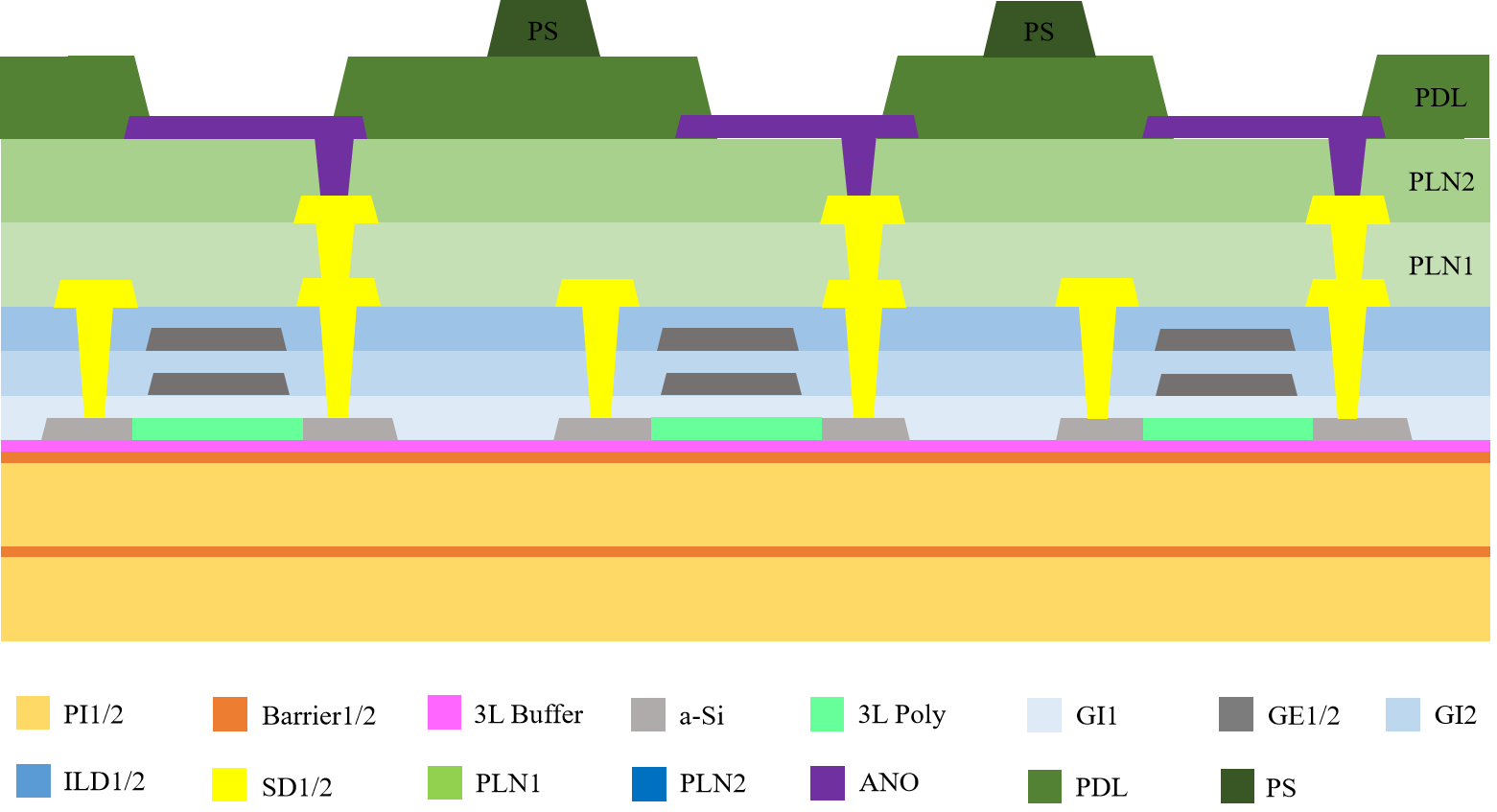
As showed in Figure 7, the PSPI was used to form PLN layer, PDL layer and PS layer in the preparation of OLED device. The PLN layer was covered on the source drain layer and used to reduce the undulating drop caused by the patterning source drain layer. The number of PLN layer was usually more than one layer, which was decided by the technological requirements of OLED device. The patterning anode of the electroluminescence (EL) part was formed on the surface of PLN layer. Then the PDL layer was covered on the PLN layer and anode layer, which was used to defined the pixel deposited area. The opening area in the PDL layer was used to deposit the luminescent functional layer during the electroluminescence (EL) manufacturing process with fine metal mask (FMM) technology. The PS layer was formed based on the technology of half tone mask technology and was used to as supporting part to prevent the anode from being damaged during the EL manufacturing process.
Figure 7.
The architecture of PSPI used in the array structure of OLED device. 2.2.2.2 The application of PSPI used in IC fabrication
As a polymer that combines photosensitive properties and high-performance material properties, PSPI is widely used in dielectric layers and passivation films in chip manufacturing.66 Its core characteristics and functions are reflected in three dimensions including material properties, process optimization and functional implementation. For the core characteristics and functions of PSPI as a dielectric layer, the high insulation and structural stability of PSPI were its key material characteristics. Base on the excellent dielectric properties, such as a typical dielectric constant of 3.0-3.5, a dielectric strength of 200-300kV/mm, a volume resistivity of 10¹⁶-10¹⁸Ω·cm and a surface resistivity of 10¹³-106¹Ω·cm, PSPI could effectively isolate electrical crosstalk between different layers of the chip. When used as dielectric layers and passivation layer in manufacturing of chip, PSPI can simplify the patterning process and reduce costs obviously. Traditional non photosensitive PI relies on photoresist to complete patterning, which includes multiple steps such as coating, curing, photoresist coating, exposure, development and etching process. While, the photosensitive groups (such as epoxy groups and double bonds) contained in PSPI structure can be directly crosslinked or decomposed through radiation such as ultraviolet light, eliminating the need for additional photoresist and etching steps, shortening the process cycle and saving material costs. The protection function of PSPI was isolating environmental erosion and improving chip reliability when using as a passivation film. The passivation film in IC structure needs to protect the surface of the chip from water vapor, impurities and chemical corrosion.67 PSPI can form a stable protective layer in high temperature and high humidity environments to reduce leakage current and increase breakdown voltage based on its dense molecular structure (main chain containing imide rings) and high temperature resistance (high Tg). For example, PSPI was used as a surface passivation layer in CPU and GPU flip chip packaging to ensure the long-term stability of precision circuits.
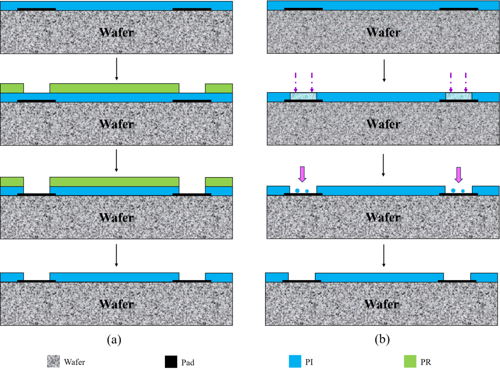
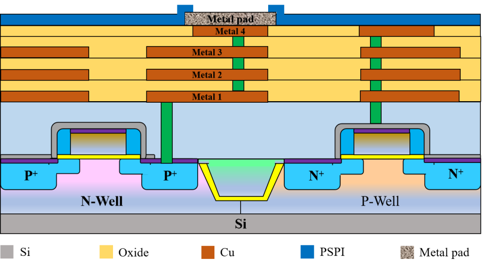
The application of PSPI in the semiconductor and microelectronics industry is mainly used as passivation layer and particle shielding film. For the passivation layer, the PSPI was usually used to form the protecting layer of the chip to prevent the IC from being damaged during the using process.68 The architecture of PSPI used as a protecting layer in logic IC was showed in Figure 8. The PAA resin solution was sprayed on a substrate directly with a spinning or slitting coating method and formed a wet organic layer which with a uniform thickness. Then a soft process was carried out to remove the most solvents of wet organic layer. The exposure and develop process were carried out to form the request patterning with a mask. Finally, the curving process was used to confirm the PSPI film sturdy. For the particle shielding film, the radiation resistance performance of IC became more important based on the increasing of integrated circuit density and chip size. The high purity polyimide film is an effective radiation and particle resistant shielding material. Forming a 50~100um radiation shielding layer on the passivation film of the component casing can prevent memory errors caused by the release of trace amounts of uranium and peony. The excellent mechanical properties of polyimide can prevent chips from breaking during subsequent packaging processes.The structure of particle shielding film usually included two types, which were oxide/nitride/PSPI layer and fully PSPI layer.
Figure 8.
The architecture of PSPI used in the fabrication of logic IC. 2.2.2.3 The application of PSPI used in IC packaging
In the manufacturing of IC packaging, PSPI has played a key role in improving packaging reliability and process efficiency by using as a stress buffer layer and adhesive based on its unique material properties. For its mechanical performance advantages, a high elastic modulus (usually 2-5GPa) and low CTE (20-50ppm/°C) of PSPI could enable it to effectively absorb thermal stress between the chip and substrate for preventing warping or cracking caused by temperature cycling. The imide ring in its molecular structure endows the PSPI with high toughness for providing cushioning protection in the event of chip drop or mechanical vibration, which was especially suitable for mobile device chip packaging.69 For the application scenarios and technological value, PSPI was used as core layer during the advanced IC packaging. For example, PSPI was served as a stress buffer layer for the rewiring layer (RDL) to isolate the thermal expansion difference between the silicon chip and the organic substrate for ensuring the stability of high-density interconnect structure in chip on wafer on substrate (CoWoS) and fan out wafer level packaging (FOWLP) technologies. When using as stress buffer layer, PSPI could also improve the lifespan of chips in high temperature and high humidity environments by reducing solder joint fatigue caused by thermal stress and the risk of packaging failure also reduced significantly.70
When using as an adhesive in IC packaging, the polar groups (such as carbonyl and amino groups) in PSPI molecules can form chemical bonds with metals (such as copper pillars and bumps) and silicon substrates for providing stable interfacial adhesion. During the integration of multi layer structure in 2.5D/3D packaging, PSPI was used for bonding chips, interposers and substrates to achieve mechanical fixation and electrical insulation integration of heterogeneous materials. Meanwhile, PSPI can directly form adhesive area patterning through exposure and development process without the additional photoresist steps and simplifying multi-layer stacking process. Some modified PSPI material can be cured below 200℃ to avoid high-temperature damage to thermal sensitive components (such as MEMS sensors). Finally, PSPI can also used assupporting multi-layer wiring and mechanical protection. In advanced IC packaging, such as WLCSP and fan out packaging, PSPI is used as a dielectric layer to construct a rewiring layer structure for supporting micro connections such as copper pillars and bumps and protecting internal circuits from physical damage.The high strength and toughness mechanical properties (such as strong impact resistance) could adapt to stress changes during chip packaging process.
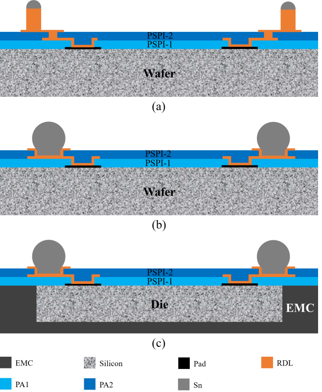
The application of PSPI used in the IC packaging is mainly used as passivation (PA) layer during the process of IC packaging. For the passivation layer, the PSPI was usually used to form the insulation layer between re-distribution layers (RDL) to block the electrical signals between the metal circuit layers of the chipeffectively, resulting no short circuits in the circuit and increasing the stability and reliability of electronic devices. Besides, the protecting layer formed by PSPI can also prevent water and oxygen from damaging the IC during the using process, which can increase the operation life of electronic devices. As showed in Figure 9a, the number of passivation layers in the IC bumping packaging was usually more than two, some electronic devices even needed three or four passivation layers. The passivation layers and RDL layers were interleaving and overlapping with each other on the surface of chips. Apart from the Cupper bump on the top layer of chip, each RDL layer was fully covered by the passivation layer to guarantee the electrical signals of chip. As showed in Figure 9b, the PSPI was also used as passivation layer in IC fan in wafer level packaging (FIWLP). The number of passivation layers in the IC FIWLP was usually less than two. The PA1 covered on the surface of chip with opening area corresponding to the pad of chip, and the patterning RDL1 also formed on the surfaces of PA1 and connected with pad of chip through the opening area in PA1. The PA2 also covered on the surface of PA1 and RDL1 with opening area, and the patterning RDL2 located on the surfaces of PA2 and connected with RDL1 through the opening area in PA2. It should be noted that the size of PA1 and PA2 were all same with the size of chip in the IC FIWLP package.As showed in Figure 9c, the PSPI was also used as passivation layer in IC fan out wafer level packaging (FOWLP). The number of passivation layers in the IC FOWLP was usually two. The PA1 covered on the surface of chip with opening area corresponding to the pad of chip, and the patterning RDL1 also formed on the surfaces of PA1 and connected with pad of chip through the opening area in PA1. The PA2 also covered on the surface of PA1 and RDL1 with opening area, and the patterning RDL2 located on the surfaces of PA2 and connected with RDL1 through the opening area in PA2. The size of PA1 and PA2 were all larger than the size of chip in the IC FOWLP package, which can provide wider area to distribute the RDL2 for meeting the increasing number of I/O density on chips.、
Figure 9.
The architecture of PSPI used as PA layer in IC packaging: (a) in bumping packaging, (b) in FIWLP packaging, (c) in FOWLP packaging.